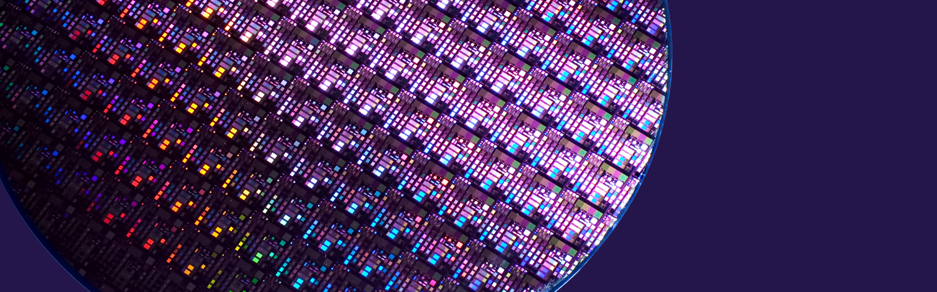
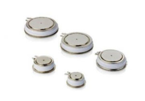
Semiconductors
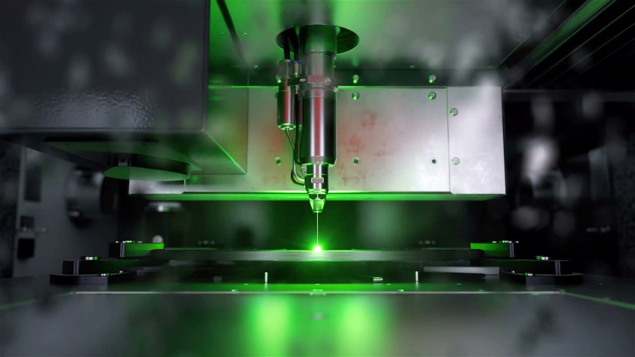
Synova’s unique water jet guided laser systems offer many advantages for applications in the semiconductor industry compared to conventional diamond blade saws or laser systems. The Laser MicroJet® combines the accuracy of a laser with the cooling and guiding capabilities of a thin water jet. This unique approach results in smooth edges, high wafer fracture strength, and less risk of breakage.
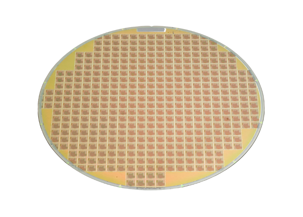
The LMJ is ideally suited for processing a wide range of semiconductor materials, including silicon (Si), gallium arsenide (GaAs), silicon carbide (SiC), low-K materials and even coated materials such as Epoxy molded compound wafers of various thicknesses. Thanks to its minimal thermal impact, the LMJ ensures that material integrity is preserved throughout the entire cutting process.
Typical semiconductor applications include wafer downsizing, wafer trimming, edge grinding, and wafer dicing. The LMJ is also used for processing semiconductor equipment and consumables, including hole drilling, slot cutting, etching, and the machining of special shapes.
Despite the limited time I could get a first in-depth insight into the LMJ potential for ablating TBC and superalloy materials. We could also identify first promising process windows for ablation at high removal rates, particularly for metals, with quality still likely to meet our typical production requirements.
The LMJ process has a particular strength in the processing of superalloy metal material. Here the benefit from the local cooling by the water jet and the tolerant focus position are real assets, allowing to realize high removal rates at good quality.
Alstom (now GE) after first LMJ machining tests
Materials
The Laser MicroJet can process a wide range of materials typically used in the semiconductor industry.
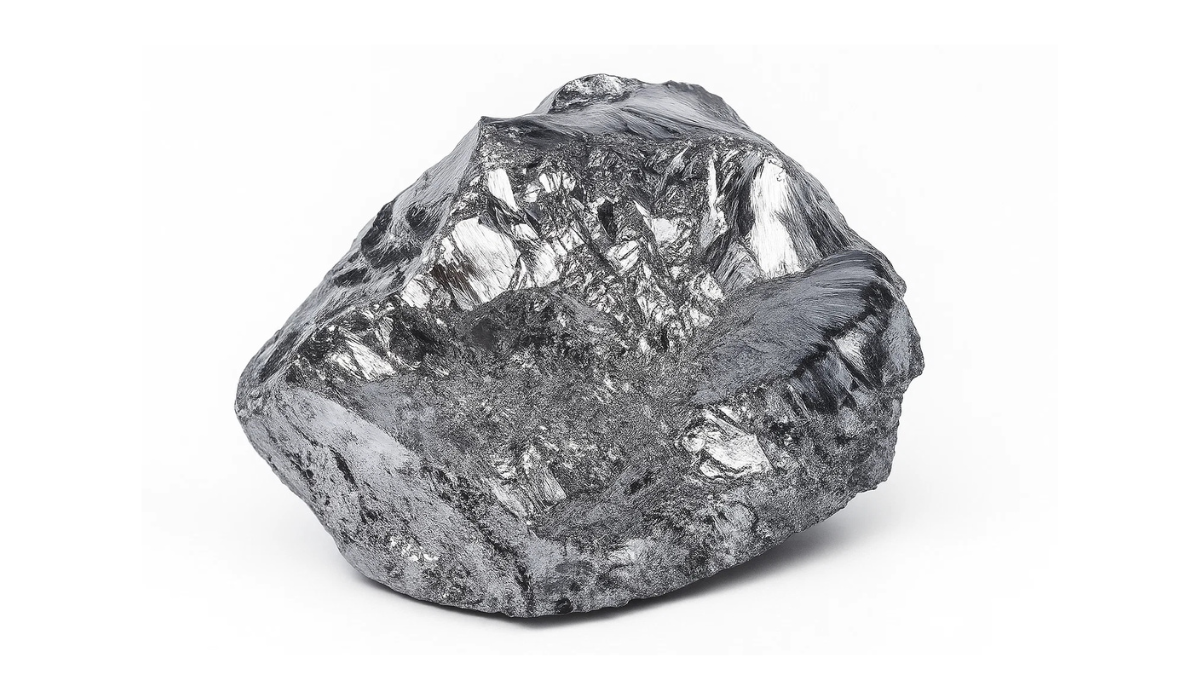
Elemental Semiconductors
Silicon (Si), Germanium (Ge), Diamond (CVD diamond)
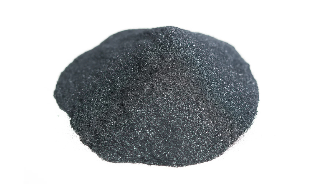
Compound Semiconductors
Silicon Carbide (SiC), Gallium Nitride (GaN), Gallium Arsenide (GaAs), Aluminum Nitride (AlN)
Application Examples
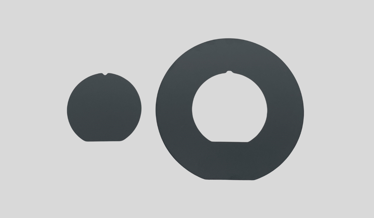
Downsizing, flat & notch
Silicon
Ingot trimming
Silicon carbide
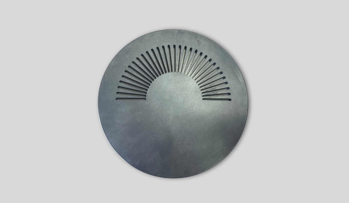
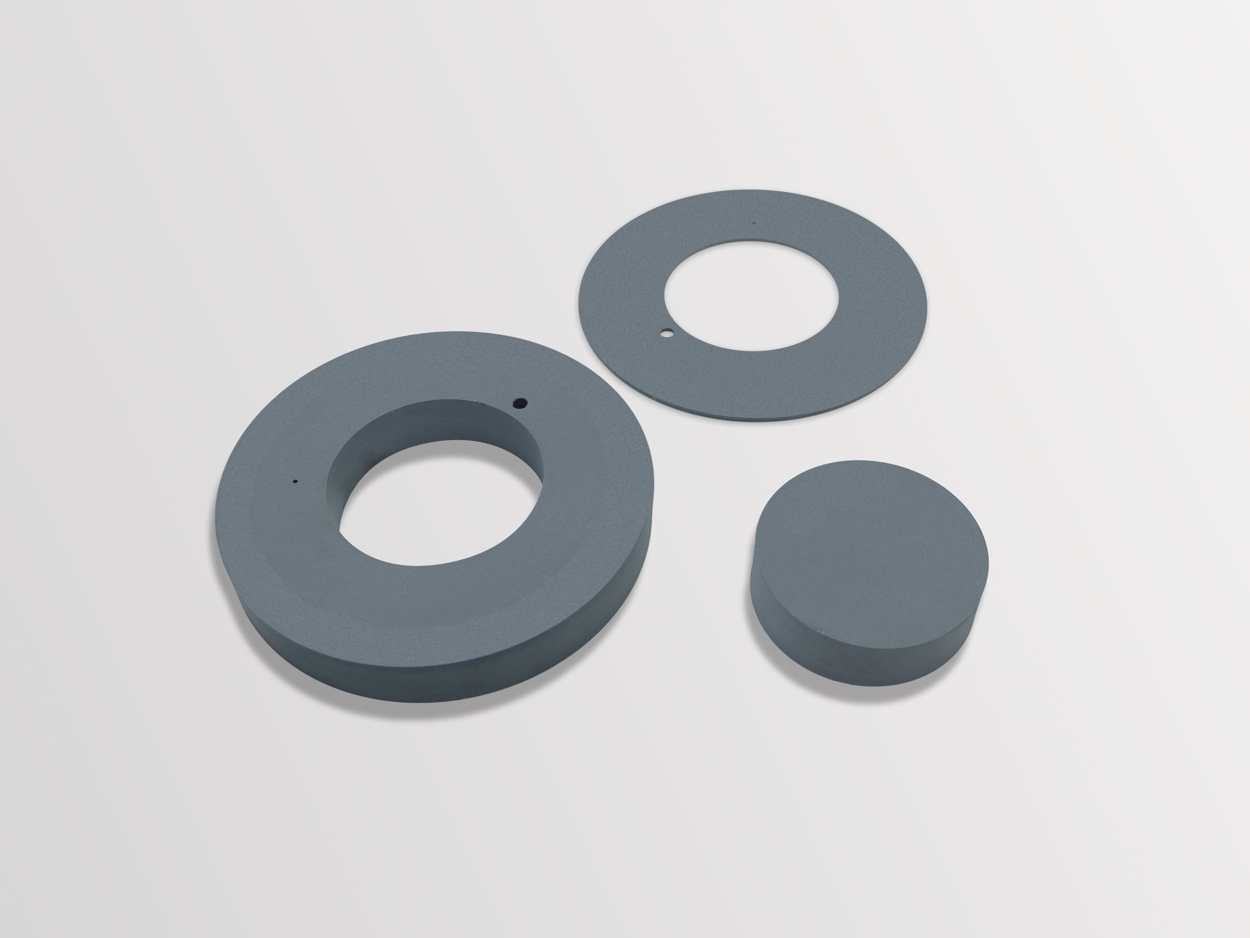
Disc slotting
Silicon
Window cutting
Black alumina
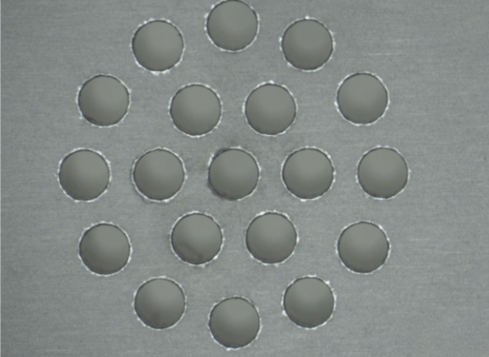
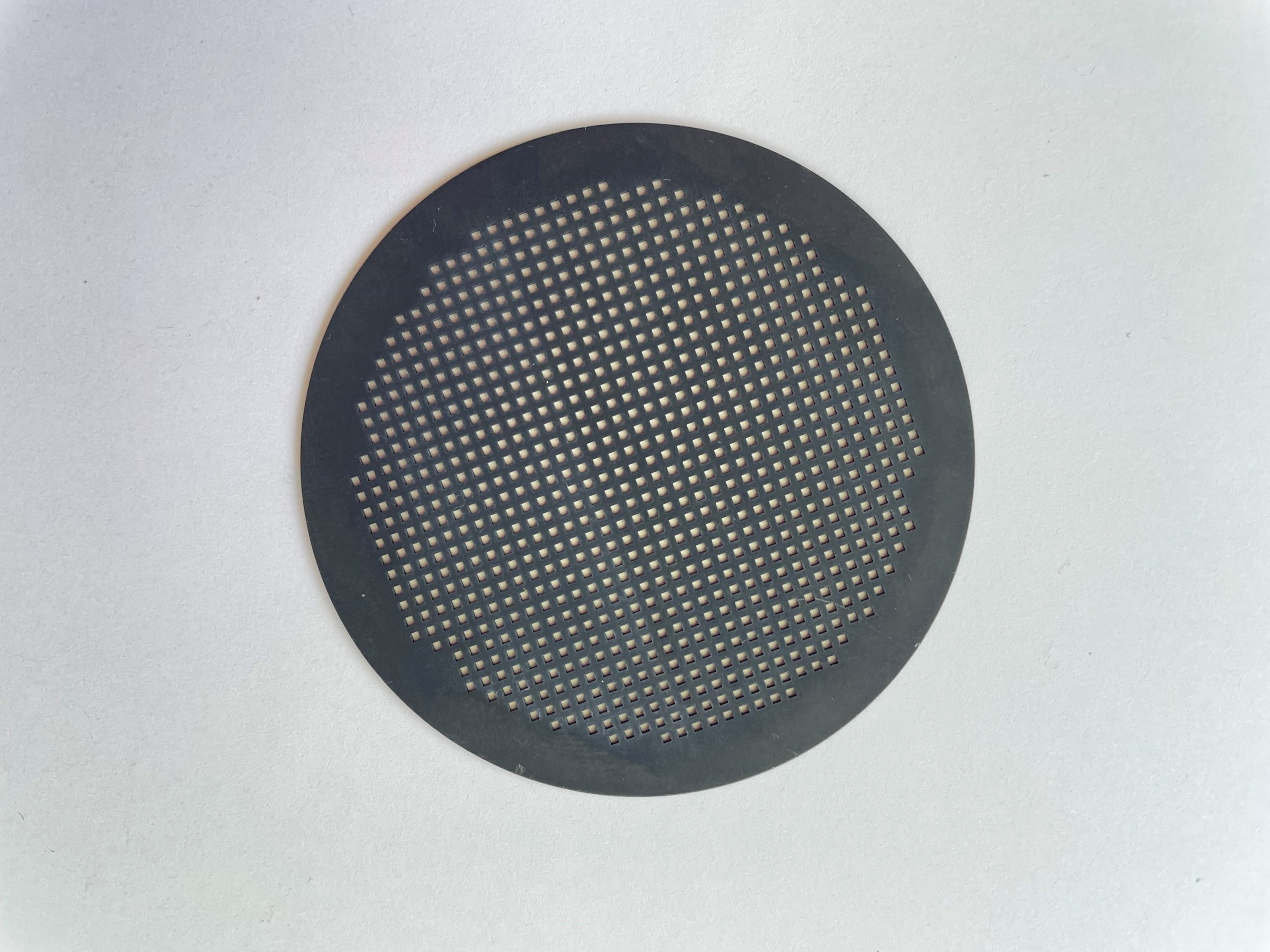
Hole drilling
Silicon carbide
Case studies
-
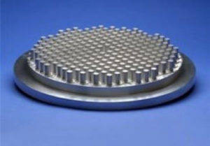
Semiconductor Reactor Sub-Assemblies
Case StudySemiconductor Reactor Sub-Assemblies
-
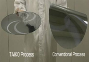
Taiko Ring Removal
Case StudyTaiko Ring Removal
-
Downsizing of Silicon Wafers
Case StudyDownsizing of Silicon Wafers
Paul Schofield
(Business Unit Manager – Semiconductors)
Meet our Business Unit Expert
Our business expert is here to support you every step of the way, whether you’re considering an application test, exploring our job shop services, or looking to discuss your upcoming production needs.